Hardware
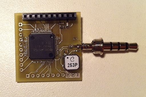
iPhone HiJack (alternative PCBs), spring 2011
Replication of the Project HiJack at the EECS Department, University of Michigan. From the project website: “Hijacking power and bandwidth from the mobile phone’s audio interface. Creating a cubic-inch peripheral sensor ecosystem for the mobile phone.” Sounds quite intriguing (but maybe it’s just easier to connect peripherals to Android phones via USB… ;-). Currently I’m still busy testing my PCBs shown below.
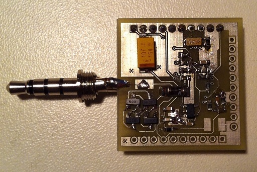
My alternative PCB version of the “HiJack” platform (front and back side). The circuit diagram and a slightly improved board layout is available here:
[zip] (Altium Designer).
I’ve basically copied the schematic and modified the PCB from the project website; my version only requires 2 layers instead of 4.
This thing actually connects to an iPhone via the audio port! The people from Michigan have uploaded a corresponding demo application on iTunes.
I’ve ordered the unpopulated printed circuit board from PCB-Pool.
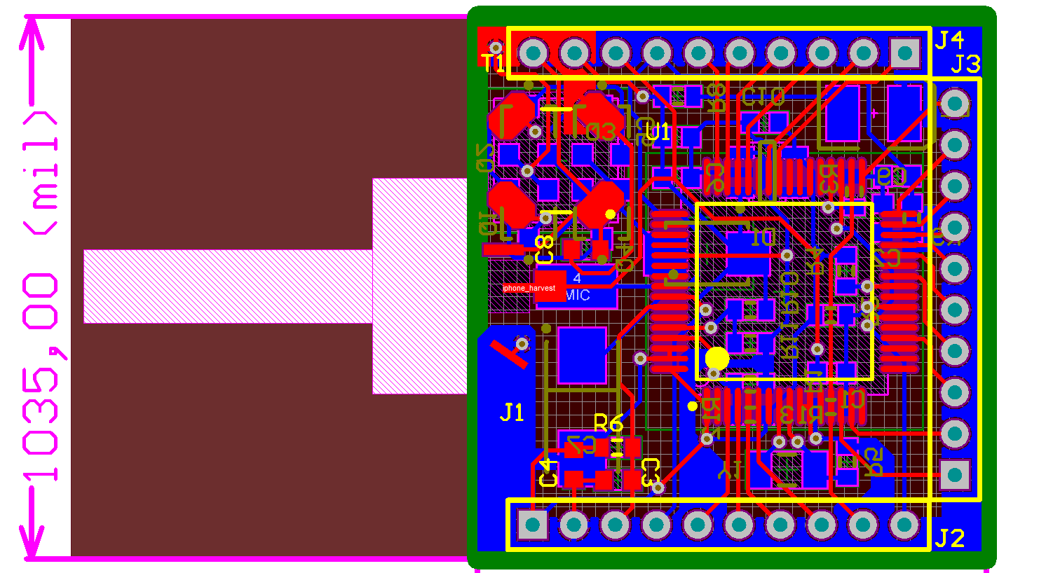
Layout preview as it appears in Altium Designer.
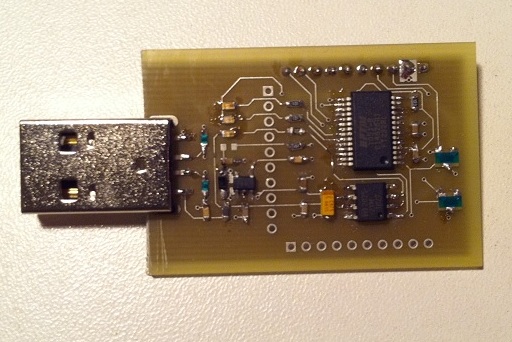

The required “programmer” for the MSP430F1611 chip at the heart of the above HiJack platform.
The programmer employs TinyOS.
My circuit diagram and board layout are available here: [zip] (Altium Designer).
This is identical to the original version, except for using Altium Designer instead of the EAGLE layout editor.
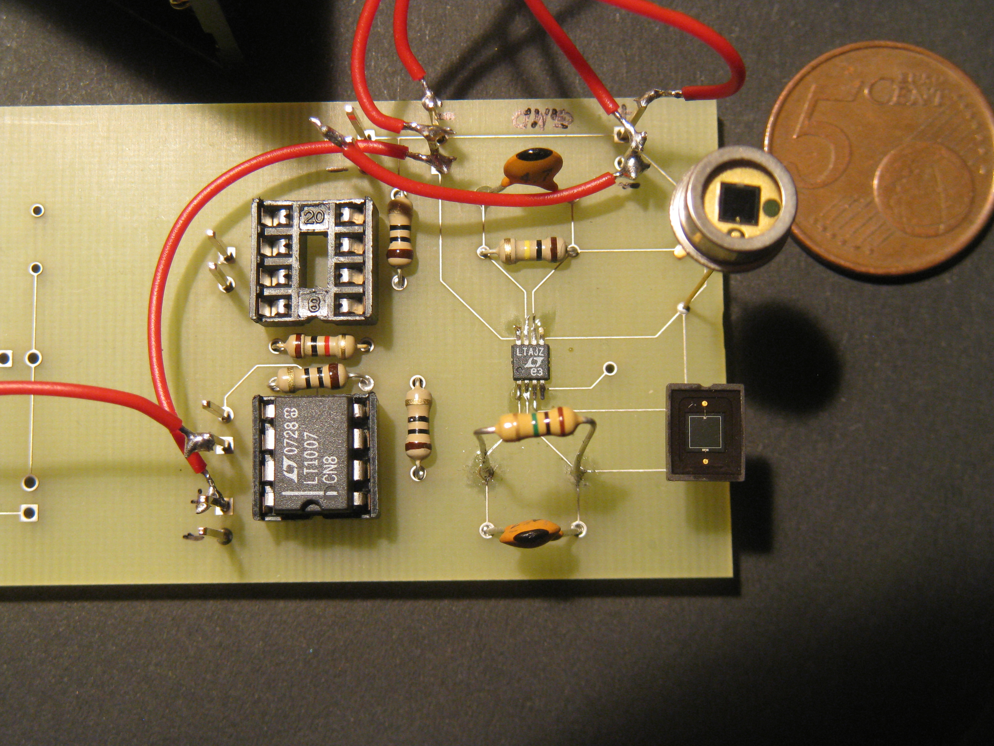
Photodiode Op-Amp, fall 2010
Here are some pictures of my attempts to construct a photodiode transimpediance amplifier. I’ve found the Electrical Engineering and Computer Science lectures from the MIT Open Courseware resources very helpful for that purpose.
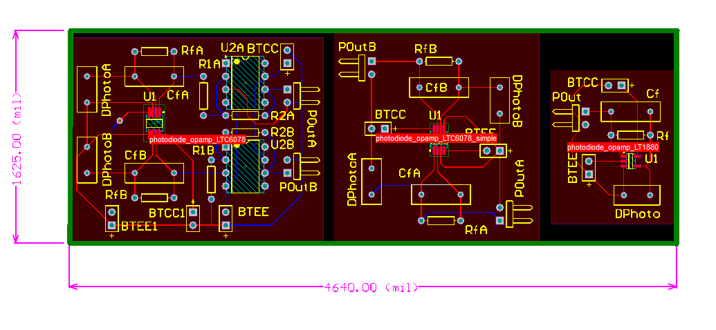
Photodiode Op-Amp circuit diagram and board layout
[zip] (Altium Designer),
layout preview [png]. Click to enlarge.
I’ve ordered the unpopulated printed circuit board from PCB-Pool.

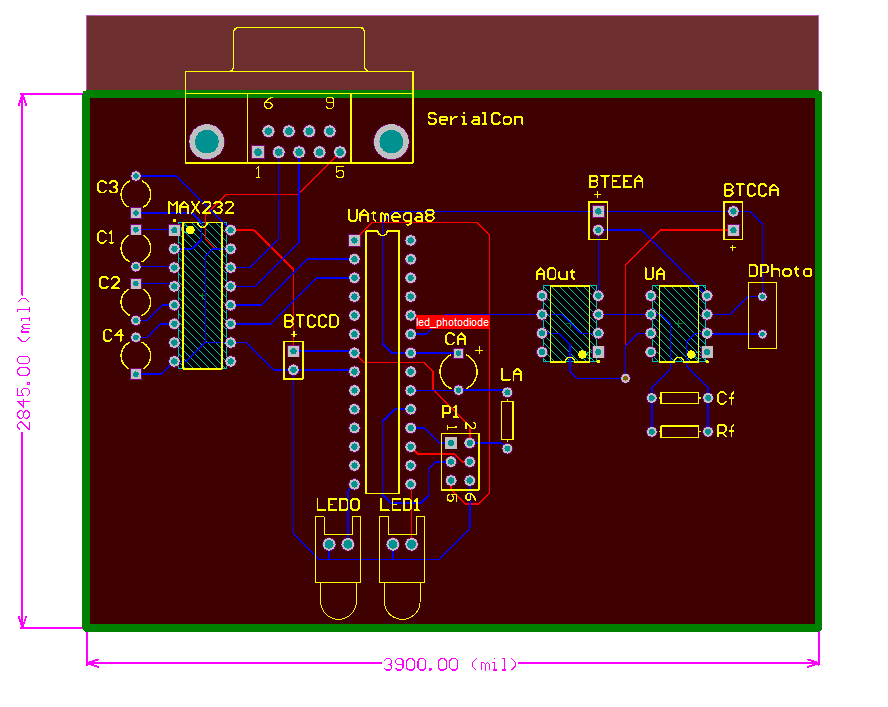
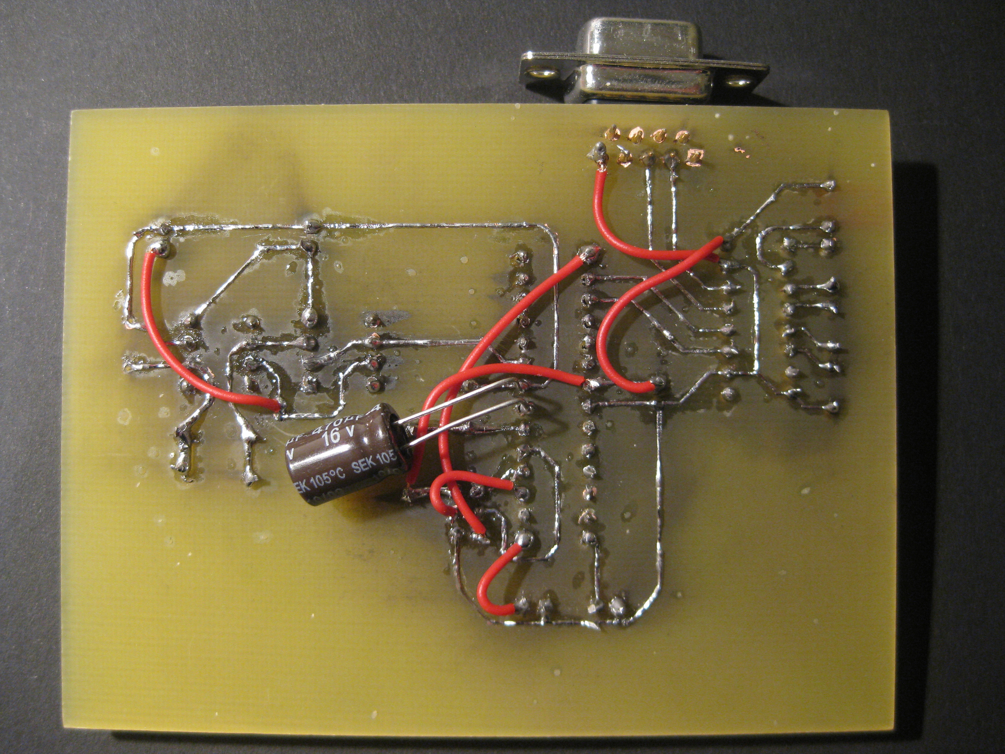
This is my current readout unit for the above Photodiode Op-Amp.
Here is the circuit diagram and board layout [zip] (Altium Designer),
and layout preview [png].
The circuit employs an
ATmega8
to accomplish the analog-to-digital data conversion. The data is transmitted to a PC via USB by the
CP2102 USB-UART bridge.
Do-It-Yourself PCBs, spring 2010
Fabricating your own PCBs sounds very intriguing… “How to make PCBs at home” has some instructions. I’ve used iron(III) chloride as etching solution.
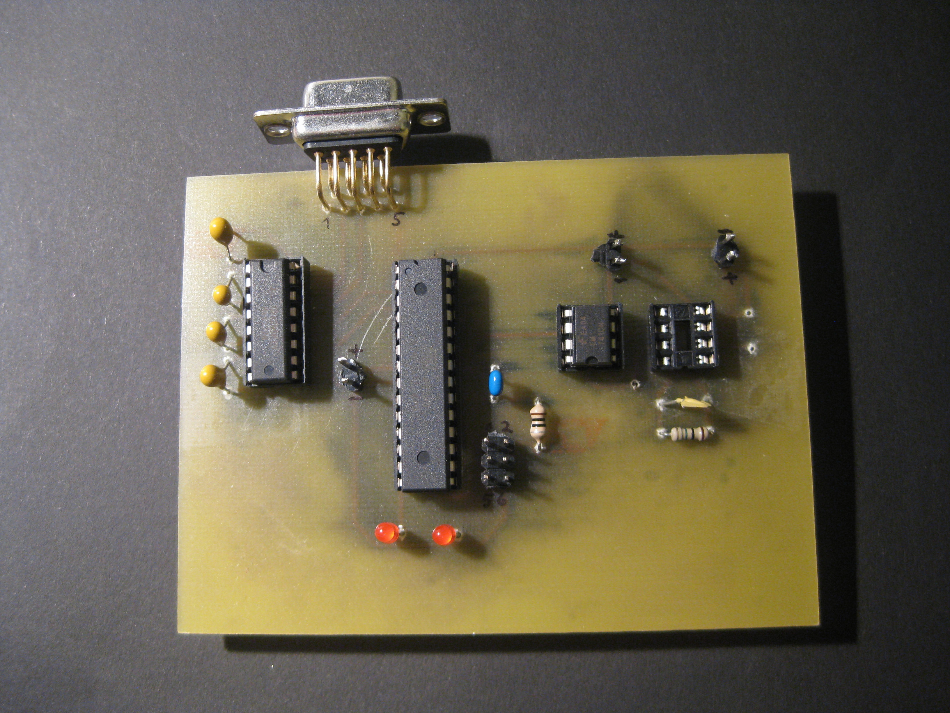
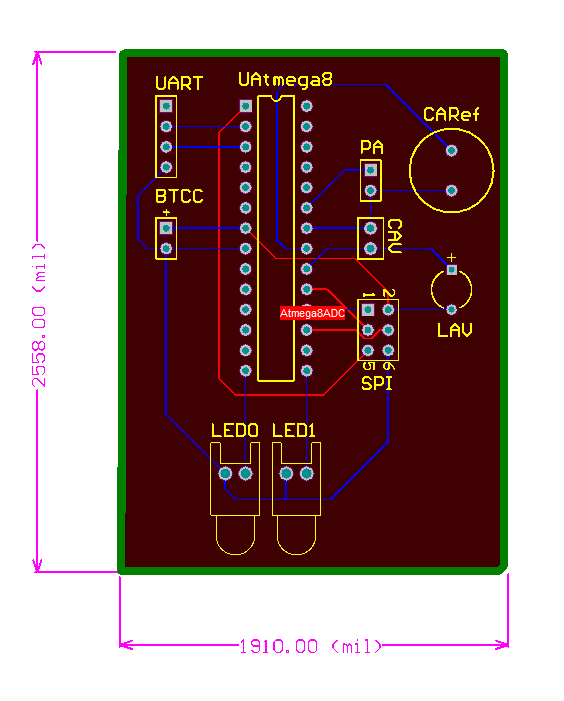
Populated “hand-made” PCB with an (obsolete) RS-232 serial port.
Circuit diagram and board layout
[zip] (Altium Designer), layout preview [png].
There is a photodiode missing since I’ve placed it into one of the boards above.
Back side of the same PCB. Doesn’t look very nice, admittedly, but works just fine!
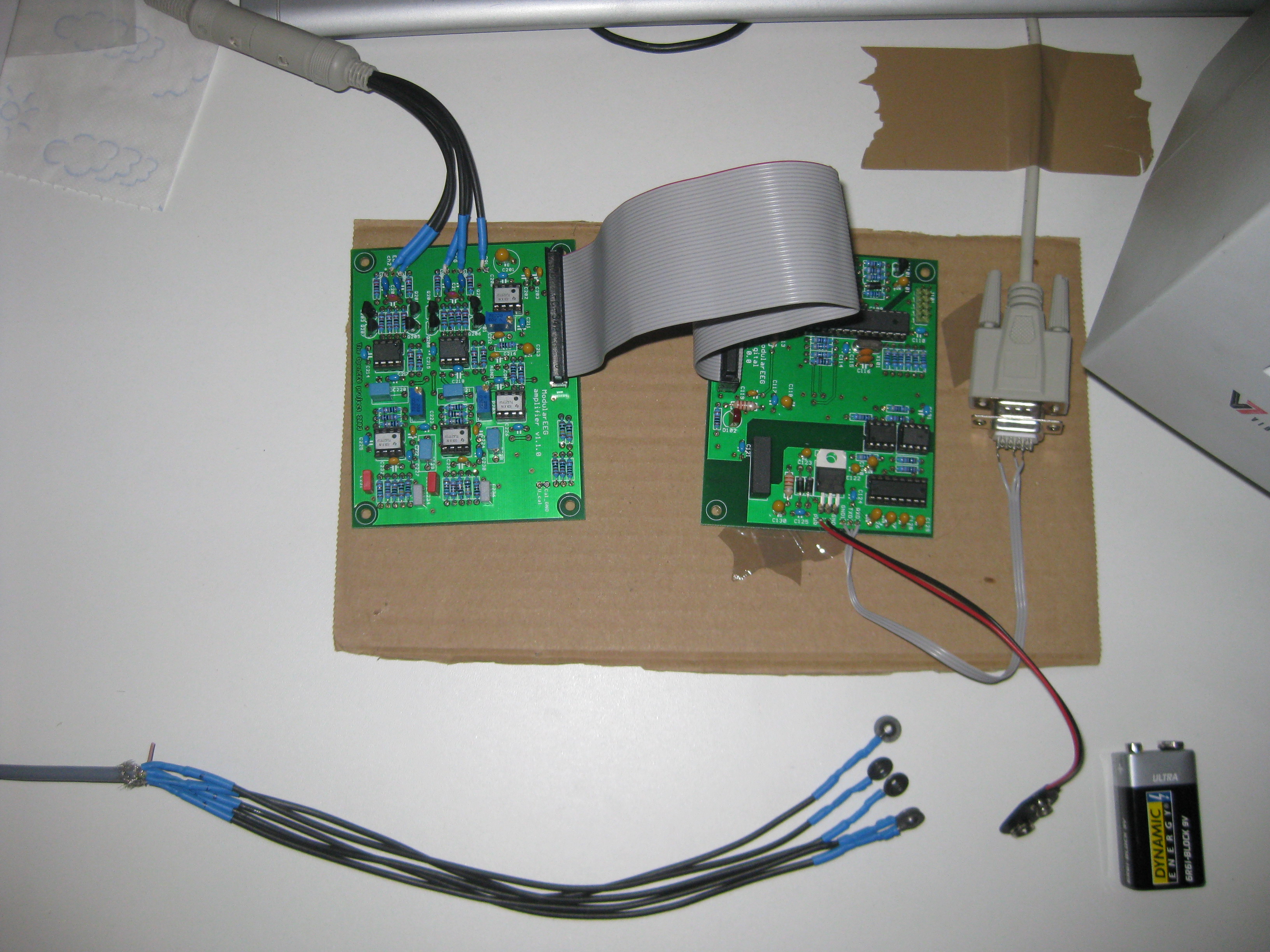
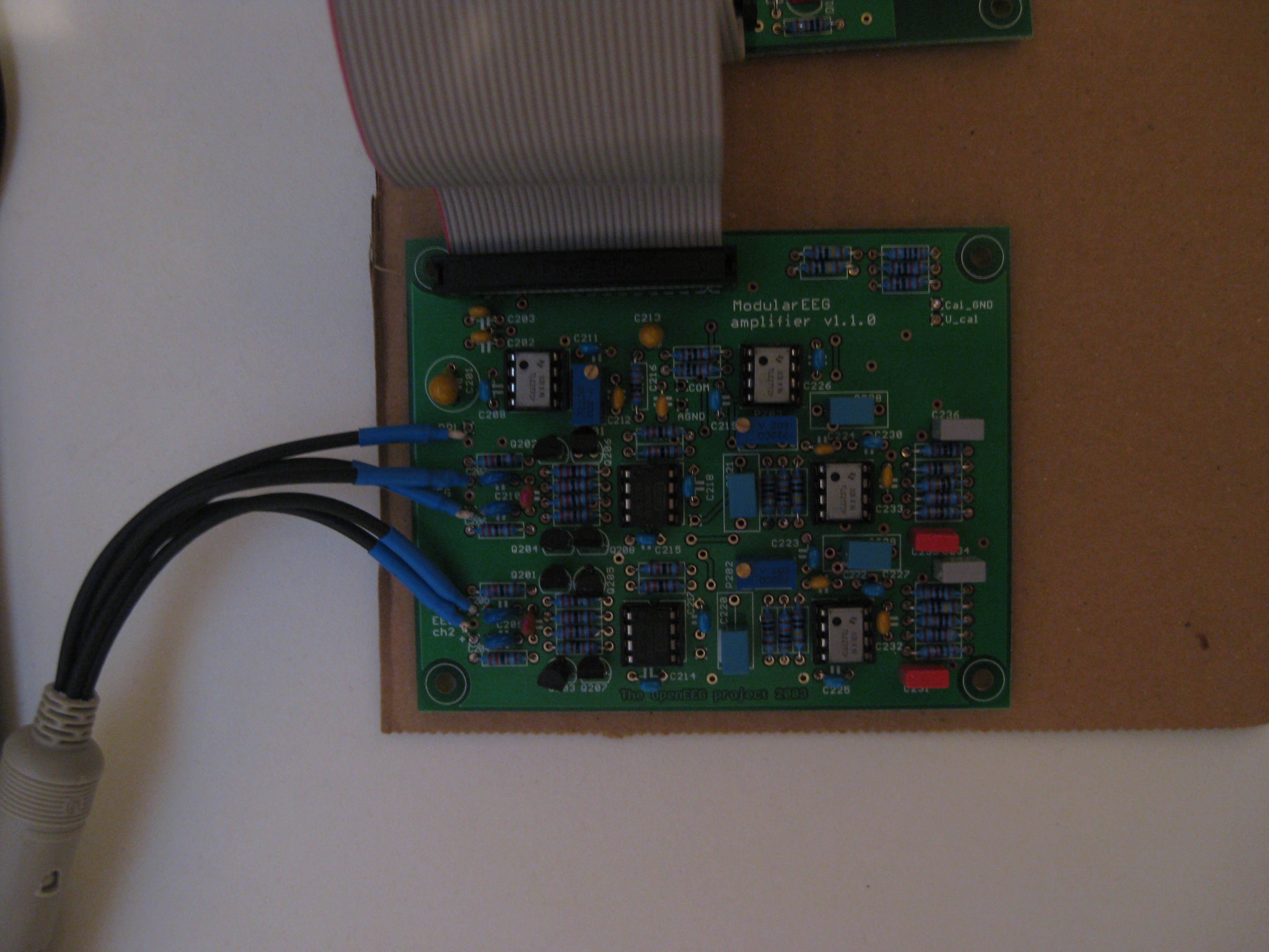
Modular EEG, spring 2009
I closely followed the instructions found at the Modular EEG project site, which aims at building a simple, two channel EEG. To the right are some screenshots of the result (click to enlarge). Soldering really took forever! I’ve ordered the bare PCBs (printed circuit boards) from Olimex and the electronic components from Reichelt, Newark and Conrad. The electrodes (10mm Ag/AgCl plastic discs) come from the “Electrode Store”. The EEG should work in principle, but I haven’t found time for testing (and actually using it…).